The provided solution is as follows:
Converting the solution to a circuit diagram retaining the orientation from the simulator would look as follows.
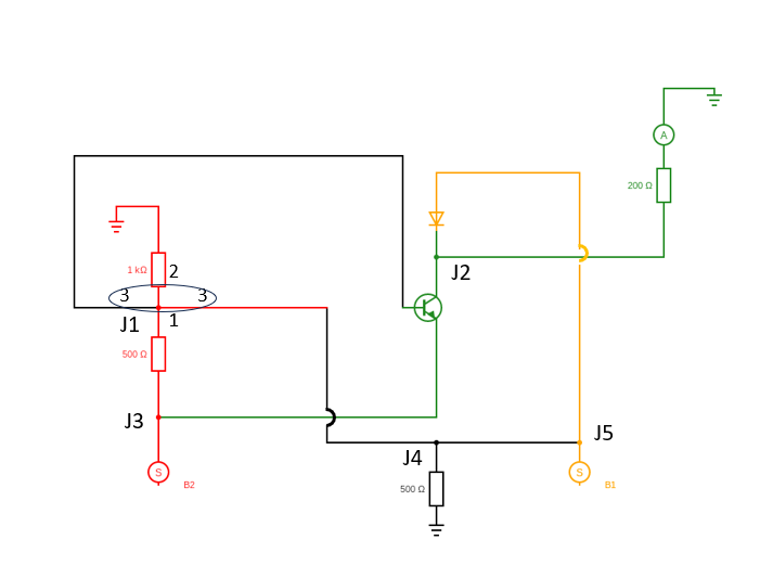
Here, a 4-way junction is included to capture the fact that T1, J1 and J4 are all in series on level 3. These can be equally well depicted as 2 virtual junctions in series connected by level 3 (see is-there-a-better-way-to-diagram-spintronic-circuits. The path from J4 to J1 can also be drawn underneath B2 to avoid a bridge in the circuit diagram.
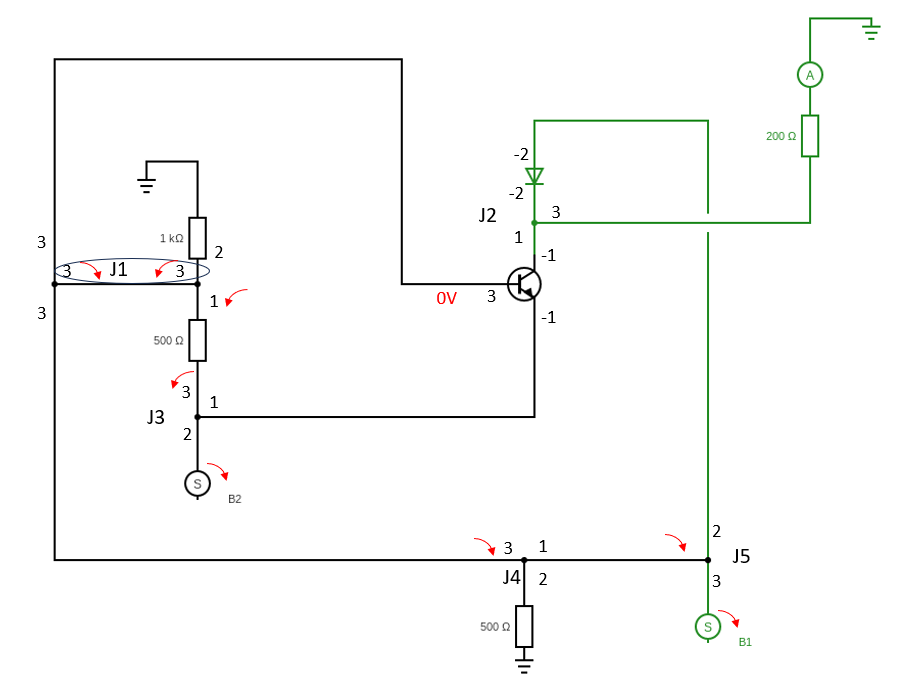
While B1 is active the current follows the green path to the Ammeter. Some of the V from B1 is tapped off at J5 going to J1 with a CW rotation ( +ve V).
B2 on the other hand has also a path to A1 (blue) but is blocked by T1. Some of the Voltage from B2 however is tapped off at J3 going to J1 with CCW rotation ( -ve V). See pic 3.
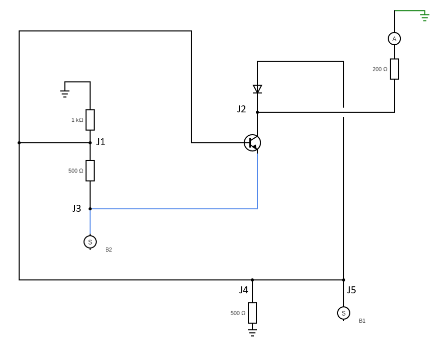
The two voltages a t J1 oppose each other. So long B1 provides a current, there is a Zero net Voltage is at J1. Therefore, the gate on T1 remains closed.
When B1 is exhausted however, J1 switches to +2V which opens the gate on T1.
Current is then free to flow from B2 to the Ammeter via the blue path (pic 4).